The LUMI Architecture
In this presentation, we will build up LUMI part by part, stressing those aspects that are important to know to run on LUMI efficiently and define jobs that can scale.
LUMI is ...
LUMI is a pre-exascale supercomputer, and not a superfast PC nor a compute cloud architecture.
Each of these architectures have their own strengths and weaknesses and offer different compromises and it is key to chose the right infrastructure for the job and use the right tools for each infrastructure.
Just some examples of using the wrong tools or infrastructure:
-
We've had users who were disappointed about the speed of a single core and were expecting that this would be much faster than their PCs. Supercomputers however are optimised for performance per Watt and get their performance from using lots of cores through well-designed software. If you want the fastest core possible, you'll need a gaming PC.
-
Even the GPU may not be that much faster for some tasks than GPUs in gaming PCs, especially since an MI250x should be treated as two GPUs for most practical purposes. The better double precision floating point operations and matrix operations, also at full precision, requires transistors also that on some other GPUs are used for rendering hardware or for single precision compute units.
-
A user complained that they did not succeed in getting their nice remote development environment to work on LUMI. The original author of these notes took a test license and downloaded a trial version. It was a very nice environment but really made for local development and remote development in a cloud environment with virtual machines individually protected by personal firewalls and was not only hard to get working on a supercomputer but also insecure.
True supercomputers, and LUMI in particular, are built for scalable parallel applications and features that are found on smaller clusters or on workstations that pose a threat to scalability are removed from the system. It is also a shred infrastructure but with a much more lightweight management layer than a cloud infrastructure and far less isolation between users, meaning that abuse by one user can have more of a negative impact on other users than in a cloud infrastructure. Supercomputers since the mid to late '80s are also build according to the principle of trying to reduce the hardware cost by using cleverly designed software both at the system and application level. They perform best when streaming data through the machine at all levels of the memory hierarchy and are not built at all for random access to small bits of data (where the definition of "small" depends on the level in the memory hierarchy).
At several points in this course you will see how this impacts what you can do with a supercomputer and how you work with a supercomputer.
LUMI spec sheet: A modular system
So we've already seen that LUMI is in the first place a EuroHPC pre-exascale machine. LUMI is built to prepare for the exascale era and to fit in the EuroHPC ecosystem. But it does not even mean that it has to cater to all pre-exascale compute needs. The EuroHPC JU tries to build systems that have some flexibility, but also does not try to cover all needs with a single machine. They are building 3 pre-exascale systems with different architecture to explore multiple architectures and to cater to a more diverse audience.
LUMI is also a very modular machine designed according to the principles explored in a series of European projects, and in particular DEEP and its successors) that explored the cluster-booster concept.
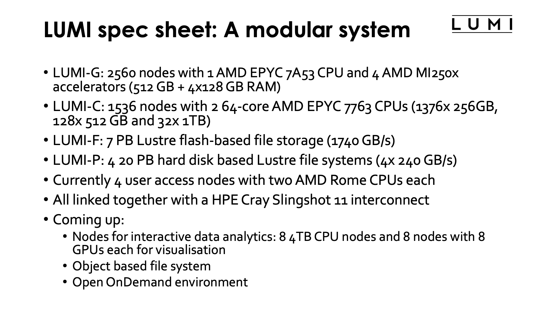
LUMI is in the first place a huge GPGPU supercomputer. The GPU partition of LUMI, called LUMI-G, contains 2560 nodes with a single 64-core AMD EPYC 7A53 CPU and 4 AMD MI250x GPUs. Each node has 512 GB of RAM attached to the CPU (the maximum the CPU can handle without compromising bandwidth) and 128 GB of HBM2e memory per GPU. Each GPU node has a theoretical peak performance of 200 TFlops in single (FP32) or double (FP64) precision vector arithmetic (and twice that with the packed FP32 format, but that is not well supported so this number is not often quoted). The matrix units are capable of about 400 TFlops in FP32 or FP64. However, compared to the NVIDIA GPUs, the performance for lower precision formats used in some AI applications is not that stellar.
LUMI also has a large CPU-only partition, called LUMI-C, for jobs that do not run well on GPUs, but also integrated enough with the GPU partition that it is possible to have applications that combine both node types. LUMI-C consists of 1536 nodes with 2 64-core AMD EPYC 7763 CPUs. 32 of those nodes have 1TB of RAM (with some of these nodes actually reserved for special purposes such as connecting to a Quantum computer), 128 have 512 GB and 1376 have 256 GB of RAM.
LUMI also has a 7 PB flash based file system running the Lustre parallel file system. This system is often denoted as LUMI-F. The bandwidth of that system is 1740 GB/s. Note however that this is still a remote file system with a parallel file system on it, so do not expect that it will behave as the local SSD in your laptop. But that is also the topic of another session in this course.
The main work storage is provided by 4 20 PB hard disk based Lustre file systems with a bandwidth of 240 GB/s each. That section of the machine is often denoted as LUMI-P.
Big parallel file systems need to be used in the proper way to be able to offer the performance that one would expect from their specifications. This is important enough that we have a separate session about that in this course.
Currently LUMI has 4 login nodes, called user access nodes in the HPE Cray world. They each have 2 64-core AMD EPYC 7742 processors and 1 TB of RAM. Note that whereas the GPU and CPU compute nodes have the Zen3 architecture code-named "Milan", the processors on the login nodes are Zen2 processors, code-named "Rome". Zen3 adds some new instructions so if a compiler generates them, that code would not run on the login nodes. These instructions are basically used in cryptography though. However, many instructions have very different latency, so a compiler that optimises specifically for Zen3 may chose another ordering of instructions then when optimising for Zen2 so it may still make sense to compile specifically for the compute nodes on LuMI.
All compute nodes, login nodes and storage are linked together through a high-performance interconnect. LUMI uses the Slingshot 11 interconnect which is developed by HPE Cray, so not the Mellanox/NVIDIA InfiniBand that you may be familiar with from many smaller clusters, and as we shall discuss later this also influences how you work on LUMI.
Some services for LUMI are still in the planning.
LUMI also has nodes for interactive data analytics. 8 of those have two 64-core Zen2/Rome CPUs with 4 TB of RAM per node, while 8 others have dual 64-core Zen2/Rome CPUs and 8 NVIDIA A40 GPUs for visualisation. Currently we are working on an Open OnDemand based service to make some fo those facilities available. Note though that these nodes are meant for a very specific use, so it is not that we will also be offering, e.g., GPU compute facilities on NVIDIA hardware, and that these are shared resources that should not be monopolised by a single user (so no hope to run an MPI job on 8 4TB nodes).
An object based file system similar to the Allas service of CSC that some of the Finnish users may be familiar with is also being worked on.
Early on a small partition for containerised micro-services managed with Kubernetes was also planned, but that may never materialize due to lack of people to set it up and manage it.
In this section of the course we will now build up LUMI step by step.
Building LUMI: The CPU AMD 7xx3 (Milan/Zen3) CPU
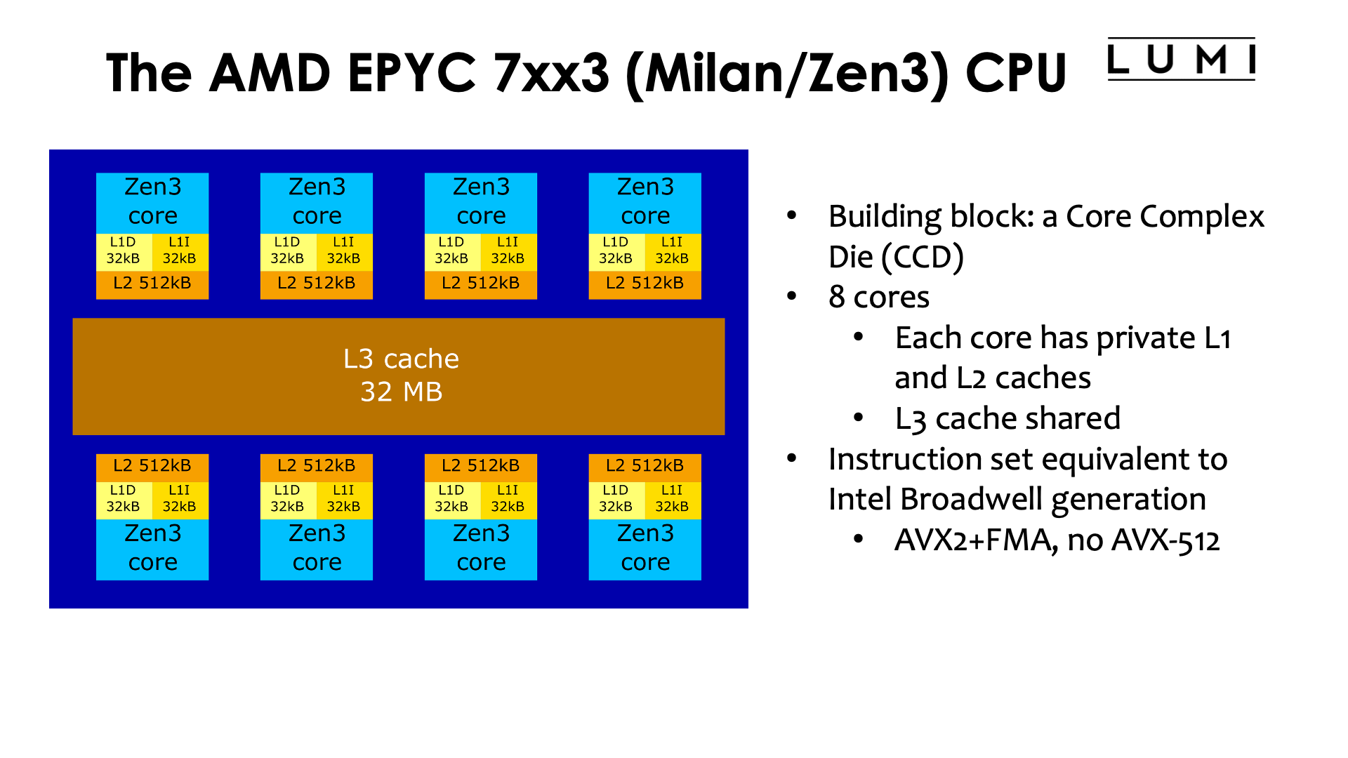
The LUMI-C and LUMI-G compute nodes use third generation AMD EPYC CPUs. Whereas Intel CPUs launched in the same period were built out of a single large monolithic piece of silicon (that only changed recently with some variants of the Sapphire Rapids CPU launched in early 2023), AMD CPUs are build out of multiple so-called chiplets.
The basic building block of Zen3 CPUs is the Core Complex Die (CCD). Each CCD contains 8 cores, and each core has 32 kB of L1 instruction and 32 kB of L1 data cache, and 512 kB of L2 cache. The L3 cache is shared across all cores on a chiplet and has a total size of 32 MB on LUMI (there are some variants of the processor where this is 96MB). At the user level, the instruction set is basically equivalent to that of the Intel Broadwell generation. AVX2 vector instructions and the FMA instruction are fully supported, but there is no support for any of the AVX-512 versions that can be found on Intel Skylake server processors and later generations. Hence the number of floating point operations that a core can in theory do each clock cycle is 16 (in double precision) rather than the 32 some Intel processors are capable of.
The full processor package for the AMD EPYC processors used in LUMI have 8 such Core Complex Dies for a total of 64 cores. The caches are not shared between different CCDs, so it also implies that the processor has 8 so-called L3 cache regions. (Some cheaper variants have only 4 CCDs, and some have CCDs with only 6 or fewer cores enabled but the same 32 MB of L3 cache per CCD).
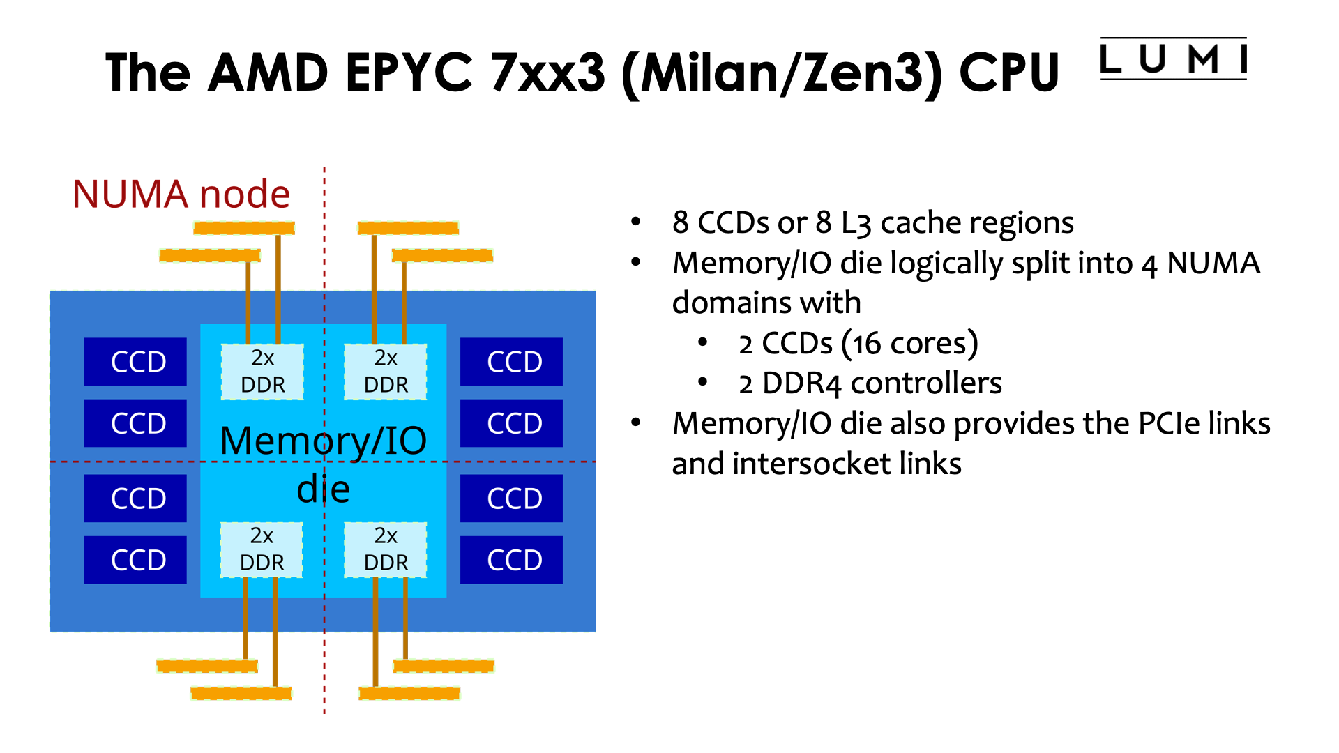
Each CCD connects to the memory/IO die through an Infinity Fabric link. The memory/IO die contains the memory controllers, connections to connect two CPU packages together, PCIe lanes to connect to external hardware, and some additional hardware, e.g., for managing the processor. The memory/IO die supports 4 dual channel DDR4 memory controllers providing a total of 8 64-bit wide memory channels. From a logical point of view the memory/IO-die is split in 4 quadrants, with each quadrant having a dual channel memory controller and 2 CCDs. They basically act as 4 NUMA domains. For a core it is slightly faster to access memory in its own quadrant than memory attached to another quadrant, though for the 4 quadrants within the same socket the difference is small. (In fact, the BIOS can be set to show only two or one NUMA domain which is advantageous in some cases, like the typical load pattern of login nodes where it is impossible to nicely spread processes and their memory across the 4 NUMA domains).
The theoretical memory bandwidth of a complete package is around 200 GB/s. However, that bandwidth is not available to a single core but can only be used if enough cores spread over all CCDs are used.
Building LUMI: a LUMI-C node
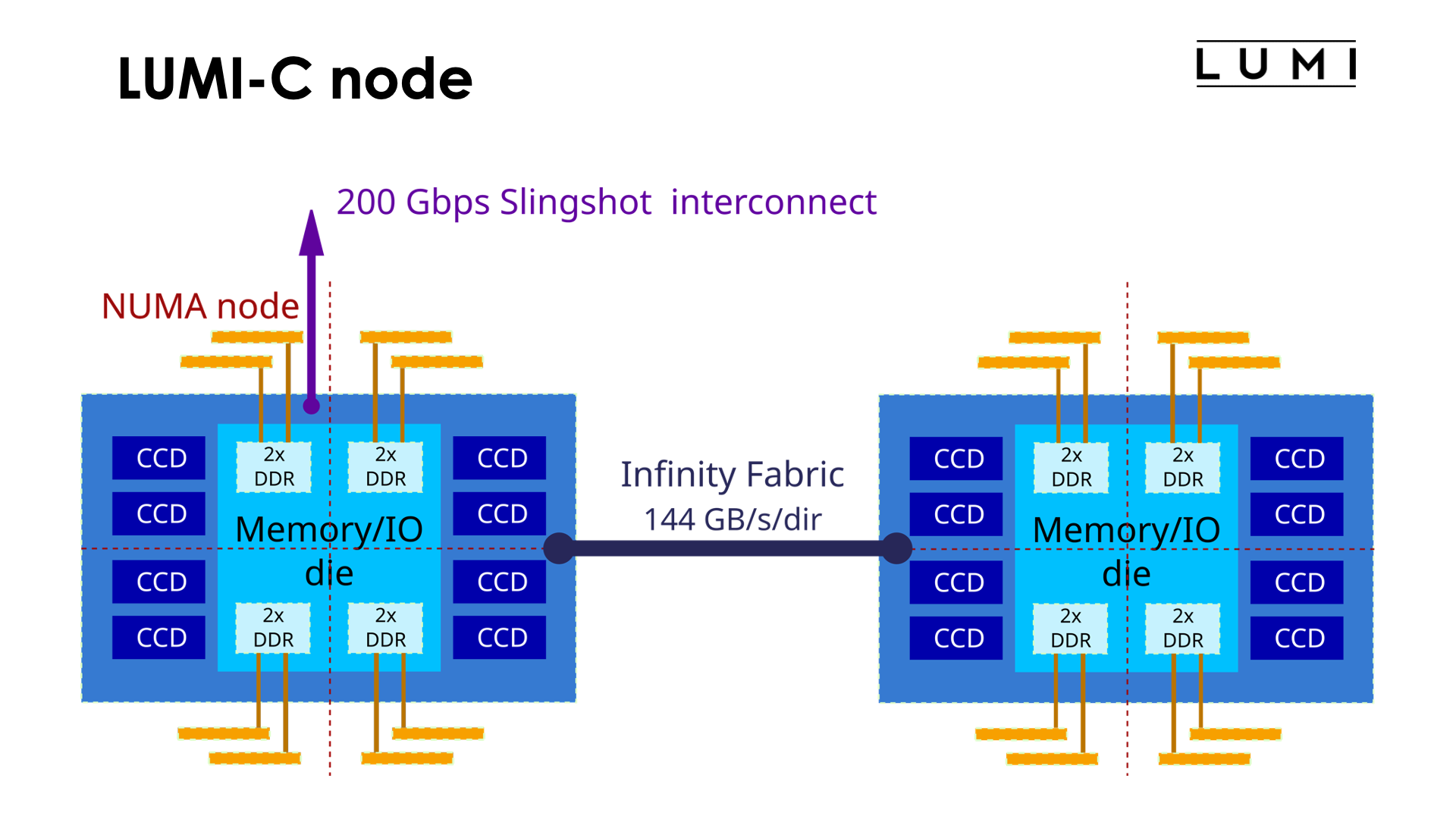
A compute node is then built out of two such processor packages, connected though 4 16-bit wide Infinity Fabric connections with a total theoretical bandwidth of 144 GB/s in each direction. So note that the bandwidth in each direction is less than the memory bandwidth of a socket. Again, it is not really possible to use the full memory bandwidth of a node using just cores on a single socket. Only one of the two sockets has a direct connection to the high performance Slingshot interconnect though.
A strong hierarchy in the node
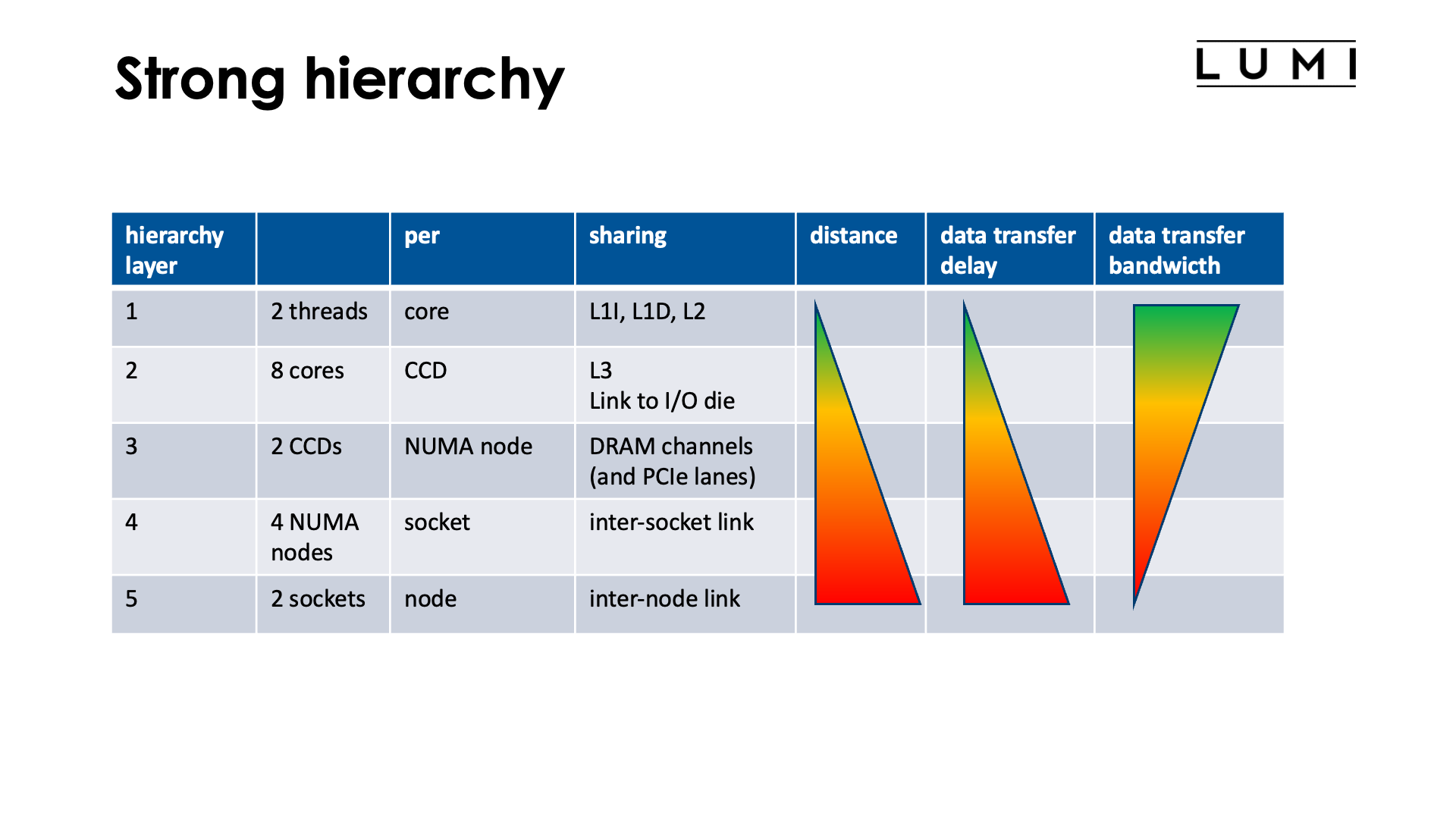
As can be seen from the node architecture in the previous slide, the CPU compute nodes have a very hierarchical architecture. When mapping an application onto one or more compute nodes, it is key for performance to take that hierarchy into account. This is also the reason why we will pay so much attention to thread and process pinning in this tutorial course.
At the coarsest level, each core supports two hardware threads (what Intel calls hyperthreads). Those hardware threads share all the resources of a core, including the L1 data and instruction caches and the L2 cache. At the next level, a Core Complex Die contains (up to) 8 cores. These cores share the L3 cache and the link to the memory/IO die. Next, as configured on the LUMI compute nodes, there are 2 Core Complex Dies in a NUMA node. These two CCDs share the DRAM channels of that NUMA node. At the fourth level in our hierarchy 4 NUMA nodes are grouped in a socket. Those 4 nodes share an inter-socket link. At the fifth and last level in our shared memory hierarchy there are two sockets in a node. On LUMI, they share a single Slingshot inter-node link.
The finer the level (the lower the number), the shorter the distance and hence the data delay is between threads that need to communicate with each other through the memory hierarchy, and the higher the bandwidth.
This table tells us a lot about how one should map jobs, processes and threads onto a node. E.g., if a process has fewer then 8 processing threads running concurrently, these should be mapped to cores on a single CCD so that they can share the L3 cache, unless they are sufficiently independent of one another, but even in the latter case the additional cores on those CCDs should not be used by other processes as they may push your data out of the cache or saturate the link to the memory/IO die and hence slow down some threads of your process. Similarly, on a 256 GB compute node each NUMA node has 32 GB of RAM (or actually a bit less as the OS also needs memory, etc.), so if you have a job that uses 50 GB of memory but only, say, 12 threads, you should really have two NuMA nodes reserved for that job as otherwise other threads or processes running on cores in those NUMA nodes could saturate some resources needed by your job. It might also be preferential to spread those 12 threads over the 4 CCDs in those 2 NUMA domains unless communication through the L3 threads would be the bottleneck in your application.
Hierarchy: delays in numbers
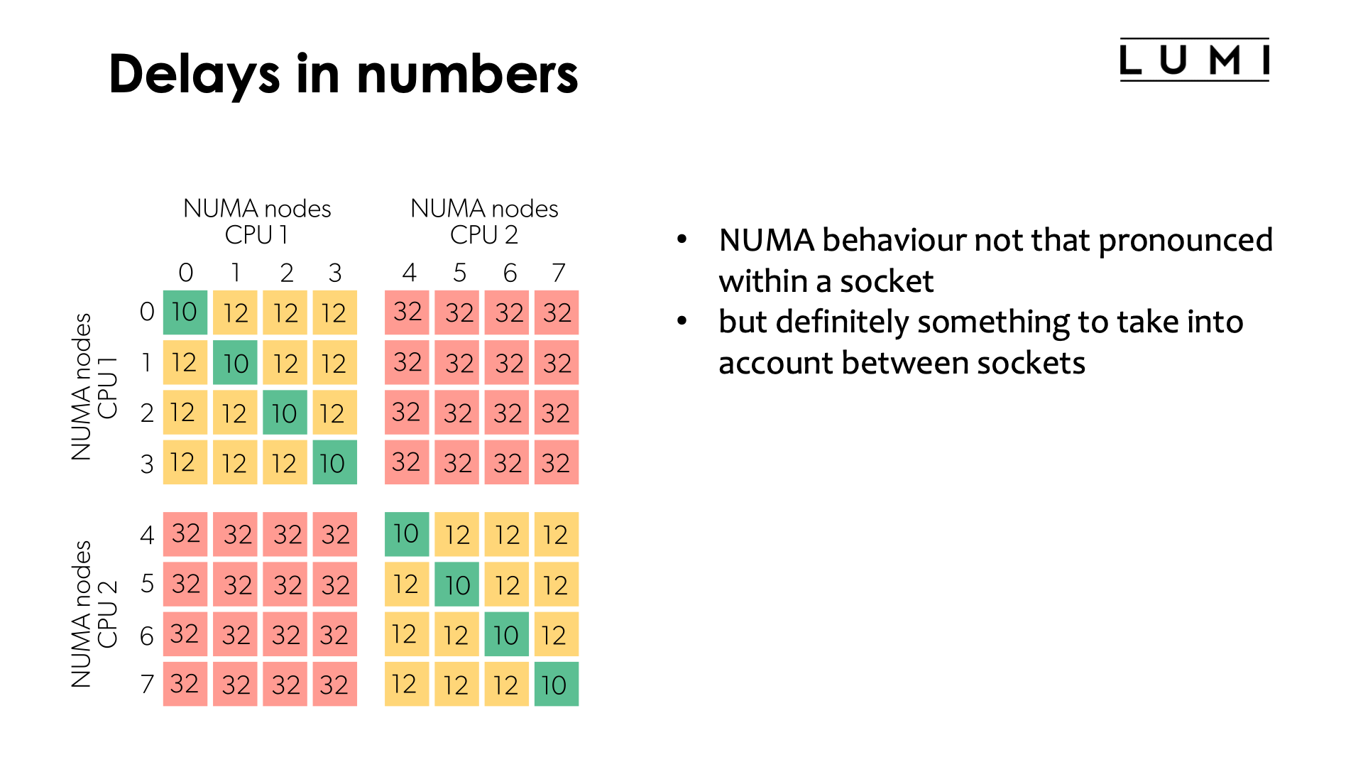
This slide shows the ACPI System Locality distance Information Table (SLIT)
as returned by, e.g., numactl -H which gives relative distances to
memory from a core. E.g., a value of 32 means that access takes 3.2x times the
time it would take to access memory attached to the same NUMA node.
We can see from this table that the penalty for accessing memory in
another NUMA domain in the same socket is still relatively minor (20%
extra time), but accessing memory attached to the other socket is a lot
more expensive. If a process running on one socket would only access memory
attached to the other socket, it would run a lot slower which is why Linux
has mechanisms to try to avoid that, but this cannot be done in all scenarios
which is why on some clusters you will be allocated cores in proportion to
the amount of memory you require, even if that is more cores than you
really need (and you will be billed for them).
Building LUMI: Concept LUMI-G node
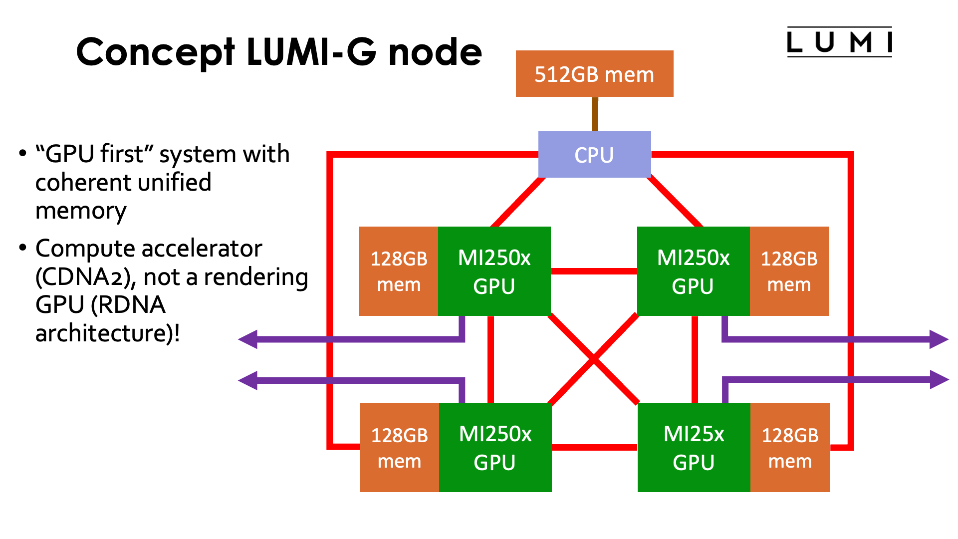
This slide shows a conceptual view of a LUMI-G compute node. This node is unlike any Intel-architecture-CPU-with-NVIDIA-GPU compute node you may have seen before, and rather mimics the architecture of the USA pre-exascale machines Summit and Sierra which have IBM POWER9 CPUs paired with NVIDIA V100 GPUs.
Each GPU node consists of one 64-core AMD EPYC CPU and 4 AMD MI250x GPUs. So far nothing special. However, two elements make this compute node very special. The GPUs are not connected to the CPU though a PCIe bus. Instead they are connected through the same links that AMD uses to link the GPUs together, or to link the two sockets in the LUMI-C compute nodes, known as xGMI or Infinity Fabric. This enables CPU and GPU to access each others memory rather seamlessly and to implement coherent caches across the whole system. The second remarkable element is that the Slingshot interface cards connect directly to the GPUs (through a PCIe interface on the GPU) rather than two the CPU. The CPUs have a shorter path to the communication network than the CPU in this design.
This makes the LUMI-G compute node really a "GPU first" system. The architecture looks more like a GPU system with a CPU as the accelerator for tasks that a GPU is not good at such as some scalar processing or running an OS, rather than a CPU node with GPU accelerator.
It is also a good fit with the cluster-booster design explored in the DEEP project series. In that design, parts of your application that cannot be properly accelerated would run on CPU nodes, while booster GPU nodes would be used for those parts that can (at least if those two could execute concurrently with each other). Different node types are mixed and matched as needed for each specific application, rather than building clusters with massive and expensive nodes that few applications can fully exploit. As the cost per transistor does not decrease anymore, one has to look for ways to use each transistor as efficiently as possible...
It is also important to realise that even though we call the partition "LUMI-G", the MI250x is not a GPU in the true sense of the word. It is not a rendering GPU, which for AMD is currently the RDNA architecture with version 3 just out, but a compute accelerator with an architecture that evolved from a GPU architecture, in this case the VEGA architecture from AMD. The architecture of the MI200 series is also known as CDNA2, with the MI100 series being just CDNA, the first version. Much of the hardware that does not serve compute purposes has been removed from the design to have more transistors available for compute. Rendering is possible, but it will be software-based rendering with some GPU acceleration for certain parts of the pipeline, but not full hardware rendering.
This is not an evolution at AMD only. The same is happening with NVIDIA GPUs and there is a reason why the latest generation is called "Hopper" for compute and "Ada Lovelace" for rendering GPUs. Several of the functional blocks in the Ada Lovelace architecture are missing in the Hopper architecture to make room for more compute power and double precision compute units. E.g., Hopper does not contain the ray tracing units of Ada Lovelace.
Graphics on one hand and HPC and AI on the other hand are becoming separate workloads for which manufacturers make different, specialised cards, and if you have applications that need both, you'll have to rework them to work in two phases, or to use two types of nodes and communicate between them over the interconnect, and look for supercomputers that support both workloads.
But so far for the sales presentation, let's get back to reality...
Building LUMI: What a LUMI-G node really looks like
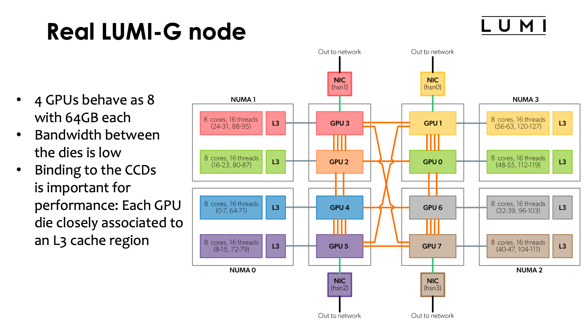
Or the full picture with the bandwidths added to it:

The LUMI-G node uses the 64-core AMD 7A53 EPYC processor, known under the code name "Trento". This is basically a Zen3 processor but with a customised memory/IO die, designed specifically for HPE Cray (and in fact Cray itself, before the merger) for the USA Coral-project to build the Frontier supercomputer, the fastest system in the world at the end of 2022 according to at least the Top500 list. Just as the CPUs in the LUMI-C nodes, it is a design with 8 CCDs and a memory/IO die.
The MI250x GPU is also not a single massive die, but contains two compute dies besides the 8 stacks of HBM2e memory, 4 stacks or 64 GB per compute die. The two compute dies in a package are linked together through 4 16-bit Infinity Fabric links. These links run at a higher speed than the links between two CPU sockets in a LUMI-C node, but per link the bandwidth is still only 50 GB/s per direction, creating a total bandwidth of 200 GB/s per direction between the two compute dies in an MI250x GPU. That amount of bandwidth is very low compared to even the memory bandwidth, which is roughly 1.6 TB/s peak per die, let alone compared to whatever bandwidth caches on the compute dies would have or the bandwidth of the internal structures that connect all compute engines on the compute die. Hence the two dies in a single package cannot function efficiently as as single GPU which is one reason why each MI250x GPU on LUMI is actually seen as two GPUs.
Each compute die uses a further 2 or 3 of those Infinity Fabric (or xGNI) links to connect to some compute dies in other MI250x packages. In total, each MI250x package is connected through 5 such links to other MI250x packages. These links run at the same 25 GT/s speed as the links between two compute dies in a package, but even then the bandwidth is only a meager 250 GB/s per direction, less than an NVIDIA A100 GPU which offers 300 GB/s per direction or the NVIDIA H100 GPU which offers 450 GB/s per direction. Each Infinity Fabric link may be twice as fast as each NVLINK 3 or 4 link (NVIDIA Ampere and Hopper respectively), offering 50 GB/s per direction rather than 25 GB/s per direction for NVLINK, but each Ampere GPU has 12 such links and each Hopper GPU 18 (and in fact a further 18 similar ones to link to a Grace CPU), while each MI250x package has only 5 such links available to link to other GPUs (and the three that we still need to discuss).
Note also that even though the connection between MI250x packages is all-to-all, the connection between GPU dies is all but all-to-all. as each GPU die connects to only 3 other GPU dies. There are basically two rings that don't need to share links in the topology, and then some extra connections. The rings are:
- 1 - 0 - 6 - 7 - 5 - 4 - 2 - 3 - 1
- 1 - 5 - 4 - 2 - 3 - 7 - 6 - 0 - 1
Each compute die is also connected to one CPU Core Complex Die (or as documentation of the node sometimes says, L3 cache region). This connection only runs at the same speed as the links between CPUs on the LUMI-C CPU nodes, i.e., 36 GB/s per direction (which is still enough for all 8 GPU compute dies together to saturate the memory bandwidth of the CPU). This implies that each of the 8 GPU dies has a preferred CPU die to work with, and this should definitely be taken into account when mapping processes and threads on a LUMI-G node.
The figure also shows another problem with the LUMI-G node: The mapping between CPU cores/dies and GPU dies is all but logical:
| GPU die | CCD | hardware threads | NUMA node |
|---|---|---|---|
| 0 | 6 | 48-55, 112-119 | 3 |
| 1 | 7 | 56-63, 120-127 | 3 |
| 2 | 2 | 16-23, 80-87 | 1 |
| 3 | 3 | 24-31, 88-95 | 1 |
| 4 | 0 | 0-7, 64-71 | 0 |
| 5 | 1 | 8-15, 72-79 | 0 |
| 6 | 4 | 32-39, 96-103 | 2 |
| 7 | 5 | 40-47, 104, 11 | 2 |
and as we shall see later in the course, exploiting this is a bit tricky at the moment.
What the future looks like...
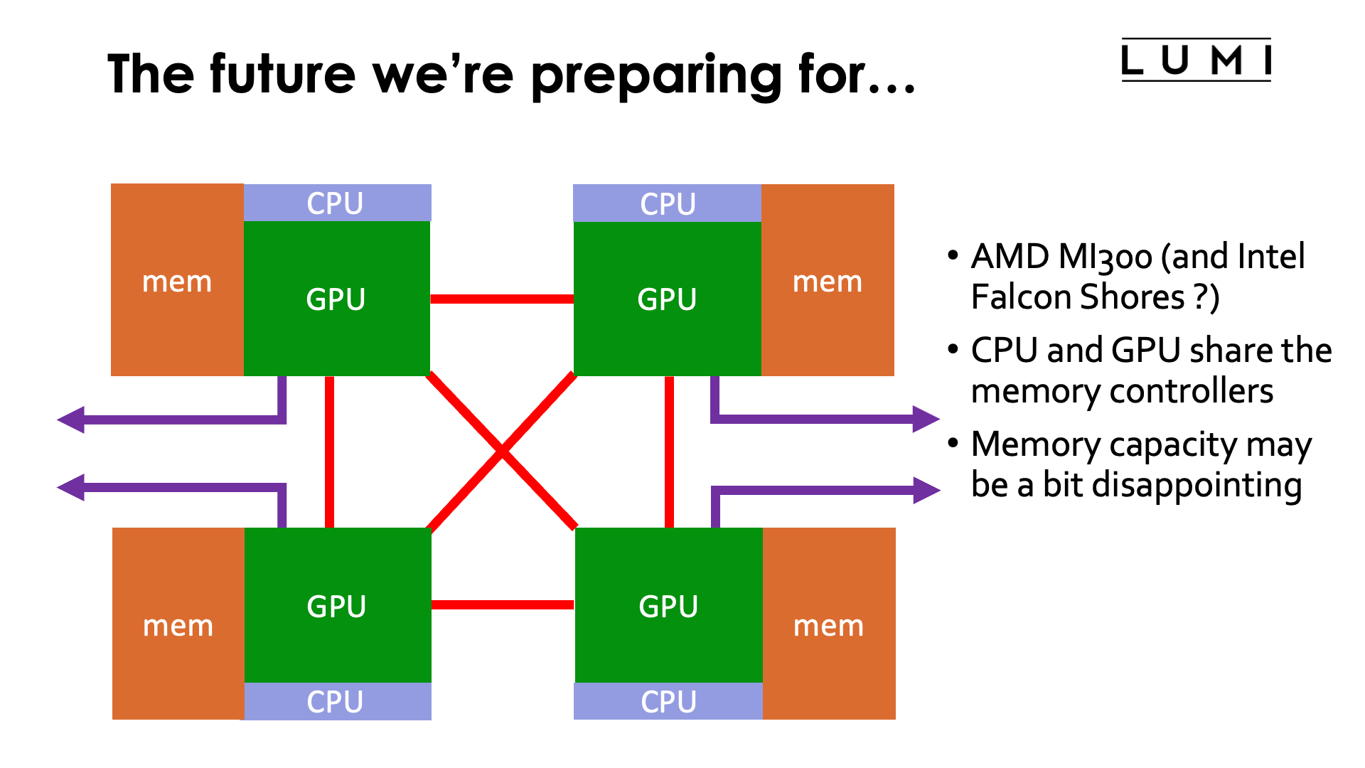
Some users may be annoyed by the "small" amount of memory on each node. Others may be annoyed by the limited CPU capacity on a node compared to some systems with NVIDIA GPUs. It is however very much in line with the cluster-booster philosophy already mentioned a few times, and it does seem to be the future according to both AMD and Intel. In fact, it looks like with respect to memory capacity things may even get worse.
We saw the first little steps of bringing GPU and CPU closer together and integrating both memory spaces in the USA pre-exascale systems Summit and Sierra. The LUMI-G node which was really designed for the first USA exascale systems continues on this philosophy, albeit with a CPU and GPU from a different manufacturer. Given that manufacturing large dies becomes prohibitively expensive in newer semiconductor processes and that the transistor density on a die is also not increasing at the same rate anymore with process shrinks, manufacturers are starting to look at other ways of increasing the number of transistors per "chip" or should we say package. So multi-die designs are here to stay, and as is already the case in the AMD CPUs, different dies may be manufactured with different processes for economical reasons.
Moreover, a closer integration of CPU and GPU would not only make programming easier as memory management becomes easier, it would also enable some code to run on GPU accelerators that is currently bottlenecked by memory transfers between GPU and CPU.
AMD at its 2022 Investor day and at CES 2023 in early January, and Intel at an Investor day in 2022 gave a glimpse of how they see the future. The future is one where one or more CPU dies, GPU dies and memory controllers are combined in a single package and - contrary to the Grace Hopper design of NVIDIA - where CPU and GPU share memory controllers. At CES 2023, AMD already showed a MI300 package that will be used in El Capitan, one of the next USA exascale systems (the third one if Aurora gets built in time). It employs 13 chiplets in two layers, linked to (still only) 8 memory stacks (albeit of a slightly faster type than on the MI250x). The 4 dies on the bottom layer are likely the controllers for memory and inter-GPU links as they produce the least heat, while it was announced that the GPU would feature 24 Zen4 cores, so the top layer consists likely of 3 CPU and 6 GPU chiplets. It looks like the AMD design may have no further memory beyond the 8 HBM stacks, likely providing 128 GB of RAM.
Intel has shown only very conceptual drawings of its Falcon Shores chip which it calls an XPU, but those drawings suggest that that chip will also support some low-bandwidth but higher capacity external memory, similar to the approach taken in some Sapphire Rapids Xeon processors that combine HBM memory on-package with DDR5 memory outside the package. Falcon Shores will be the next generation of Intel GPUs for HPC, after Ponte Vecchio which will be used in the Aurora supercomputer. It is currently not clear though if Intel will already use the integrated CPU+GPU model for the Falcon Shores generation or if this is getting postponed.
However, a CPU closely integrated with accelerators is nothing new as Apple Silicon is rumoured to do exactly that in its latest generations, including the M-family chips.
Building LUMI: The Slingshot interconnect
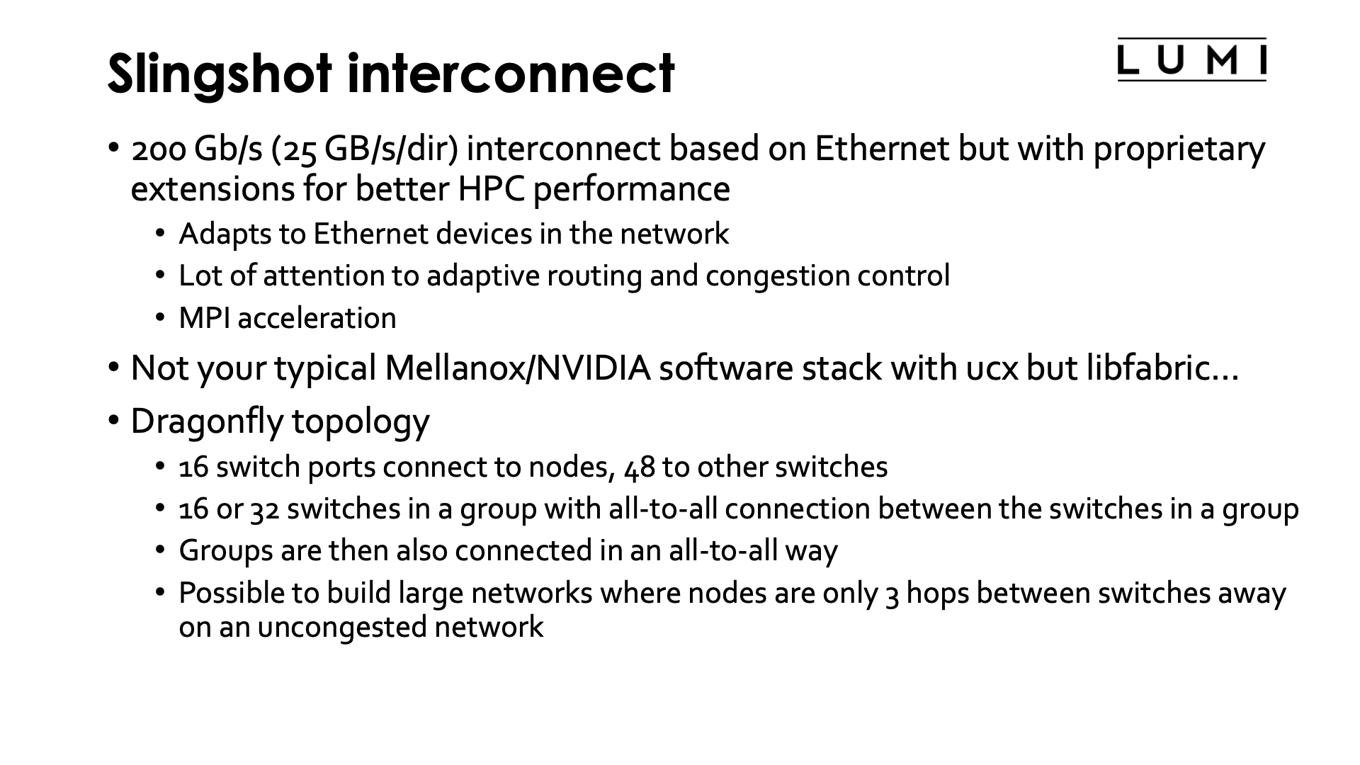
All nodes of LUMI, including the login, management and storage nodes, are linked together using the Slingshot interconnect (and almost all use Slingshot 11, the full implementation with 200 Gb/s bandwidth per direction).
Slingshot is an interconnect developed by HPE Cray and based on Ethernet, but with proprietary extensions for better HPC performance. It adapts to the regular Ethernet protocols when talking to a node that only supports Ethernet, so one of the attractive features is that regular servers with Ethernet can be directly connected to the Slingshot network switches. HPE Cray has a tradition of developing their own interconnect for very large systems. As in previous generations, a lot of attention went to adaptive routing and congestion control. There are basically two versions of it. The early version was named Slingshot 10, ran at 100 Gb/s per direction and did not yet have all features. It was used on the initial deployment of LUMI-C compute nodes but has since been upgraded to the full version. The full version with all features is called Slingshot 11. It supports a bandwidth of 200 Gb/s per direction, comparable to HDR InfiniBand with 4x links.
Slingshot is a different interconnect from your typical Mellanox/NVIDIA InfiniBand implementation and hence also has a different software stack. This implies that there are no UCX libraries on the system as the Slingshot 11 adapters do not support that. Instead, the software stack is based on libfabric (as is the stack for many other Ethernet-derived solutions and even Omni-Path has switched to libfabric under its new owner).
LUMI uses the dragonfly topology. This topology is designed to scale to a very large number of connections while still minimizing the amount of long cables that have to be used. However, with its complicated set of connections it does rely on adaptive routing and congestion control for optimal performance more than the fat tree topology used in many smaller clusters. It also needs so-called high-radix switches. The Slingshot switch, code-named Rosetta, has 64 ports. 16 of those ports connect directly to compute nodes (and the next slide will show you how). Switches are then combined in groups. Within a group there is an all-to-all connection between switches: Each switch is connected to each other switch. So traffic between two nodes of a group passes only via two switches if it takes the shortest route. However, as there is typically only one 200 Gb/s direct connection between two switches in a group, if all 16 nodes on two switches in a group would be communicating heavily with each other, it is clear that some traffic will have to take a different route. In fact, it may be statistically better if the 32 involved nodes would be spread more evenly over the group, so topology based scheduling of jobs and getting the processes of a job on as few switches as possible may not be that important on a dragonfly Slingshot network. The groups in a slingshot network are then also connected in an all-to-all fashion, but the number of direct links between two groups is again limited so traffic again may not always want to take the shortest path. The shortest path between two nodes in a dragonfly topology never involves more than 3 hops between switches (so 4 switches): One from the switch the node is connected to the switch in its group that connects to the other group, a second hop to the other group, and then a third hop in the destination group to the switch the destination node is attached to.
Assembling LUMI
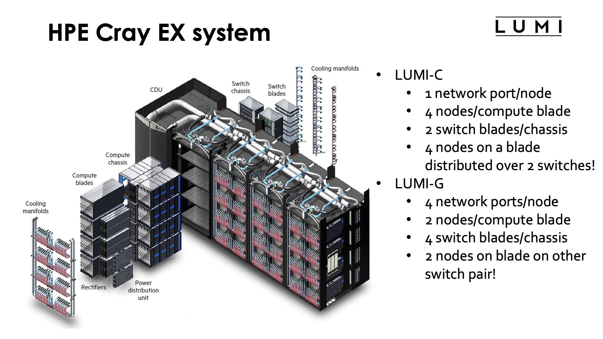
Let's now have a look at how everything connects together to the supercomputer LUMI. LUMI does use a custom rack design for the compute nodes that is also fully water cooled. It is build out of units that can contain up to 4 custom cabinets, and a cooling distribution unit (CDU). The size of the complex as depicted in the slide is approximately 12 m2. Each cabinet contains 8 compute chassis in 2 columns of 4 rows. In between the two columns is all the power circuitry. Each compute chassis can contain 8 compute blades that are mounted vertically. Each compute blade can contain multiple nodes, depending on the type of compute blades. HPE Cray have multiple types of compute nodes, also with different types of GPUs. In fact, the Aurora supercomputer which uses Intel CPUs and GPUs and El Capitan, which uses the MI300 series of APU (integrated CPU and GPU) will use the same design with a different compute blade. Each LUMI-C compute blade contains 4 compute nodes and two network interface cards, with each network interface card implementing two Slingshot interfaces and connecting to two nodes. A LUMI-G compute blade contains two nodes and 4 network interface cards, where each interface card now connects to two GPUs in the same node. All connections for power, management network and high performance interconnect of the compute node are at the back of the compute blade. At the front of the compute blades one can find the connections to the cooling manifolds that distribute cooling water to the blades. One compute blade of LUMI-G can consume up to 5kW, so the power density of this setup is incredible, with 40 kW for a single compute chassis.
The back of each cabinet is equally genius. At the back each cabinet has 8 switch chassis, each matching the position of a compute chassis. The switch chassis contains the connection to the power delivery system and a switch for the management network and has 8 positions for switch blades. These are mounted horizontally and connect directly to the compute blades. Each slingshot switch has 8x2 ports on the inner side for that purpose, two for each compute blade. Hence for LUMI-C two switch blades are needed in each switch chassis as each blade has 4 network interfaces, and for LUMI-G 4 switch blades are needed for each compute chassis as those nodes have 8 network interfaces. Note that this also implies that the nodes on the same compute blade of LUMI-C will be on two different switches even though in the node numbering they are numbered consecutively. For LUMI-G both nodes on a blade will be on a different pair of switches and each node is connected to two switches. Thw switch blades are also water cooled (each one can consume up to 250W). No currently possible configuration of the Cray EX system needs that all switch positions in the switch chassis.
This does not mean that the extra positions cannot be useful in the future. If not for an interconnect, one could, e.g., export PCIe ports to the back and attach, e.g., PCIe-based storage via blades as the switch blade environment is certainly less hostile to such storage than the very dense and very hot compute blades.
LUMI assembled
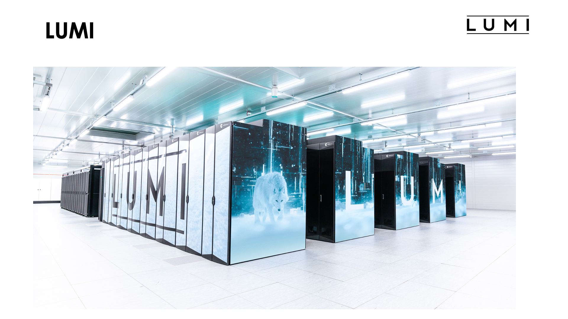
This slide shows LUMI fully assembled (as least as it was at the end of 2022).
At the front there are 5 rows of cabinets similar to the ones in the exploded Cray EX picture on the previous slide. Each row has 2 CDUs and 6 cabinets with compute nodes. The first row, the one with the wolf, contains all nodes of LUMI-C, while the other four rows, with the letters of LUMI, contain the GPU accelerator nodes. At the back of the room there are more regular server racks that house the storage, management nodes, some special compute nodes , etc. The total size is roughly the size of a tennis court.
Remark
The water temperature that a system like the Cray EX can handle is so high that in fact the water can be cooled again with so-called "free cooling", by just radiating the heat to the environment rather than using systems with compressors similar to air conditioning systems, especially in regions with a colder climate. The LUMI supercomputer is housed in Kajaani in Finland, with moderate temperature almost year round, and the heat produced by the supercomputer is fed into the central heating system of the city, making it one of the greenest supercomputers in the world as it is also fed with renewable energy.